Ver categorias
Explorar
Fiverr Pro
Português
$
USD
Designer de PCB
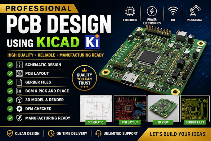
Procurando por uma PCB limpa e profissional no KiCad?
Vou criar sua PCB a partir do seu esquema, diagrama de circuito ou requisitos do projeto, com posicionamento adequado dos componentes, roteamento e verificação do projeto.
O que eu ofereço:
Pacotes:
Por favor, entre em contato antes de fazer o pedido para requisitos complexos, de alta velocidade, RF ou PCB especiais.
Vamos transformar seu circuito em uma PCB limpa e pronta para fabricação.


Tradução automática
O que você precisa para iniciar o projeto?
Preciso do seu esquema, diagrama de circuito, lista de componentes, datasheets ou quaisquer arquivos do projeto disponíveis e requisitos da PCB.
Você fornece arquivos Gerber e Drill?
Sim. Arquivos Gerber e Drill prontos para fabricação estão incluídos nos pacotes.
Você pode criar footprints personalizados?
Sim. Posso criar ou modificar footprints no KiCad quando um footprint de componente necessário não estiver disponível.
Você pode trabalhar com projetos existentes no KiCad?
Sim. Posso modificar, melhorar, roteirizar ou completar um esquema ou layout de PCB existente no KiCad.
Você consegue lidar com projetos complexos de PCB?
Sim, incluindo placas com maior número de camadas. Para requisitos avançados como controle de impedância, sinais de alta velocidade, RF ou HDI, entre em contato primeiro para uma cotação personalizada.
Você pode escolher componentes para meu projeto?
Sim. A seleção de componentes pode ser discutida dependendo dos requisitos do projeto e do escopo do pacote.