t
tomvbloghat

Felix Wagner

@tomvbloghat

Professional PCB Designer '' Altium, KiCad and EasyEDA

Alemanha
Alemão, Inglês, Holandês
Algumas informações são exibidas no idioma inglês.
Sobre mim
I’m a professional PCB Designer specialising in PCB layout, schematic design and circuit board routing. I create accurate, organised and manufacturing-ready PCB designs for prototypes and electronic products. My services include 2-layer and multilayer PCB design, component placement, PCB routing, Gerber files, drill files, BOM preparation, DRC and DFM checks. I work with Altium Designer, KiCad and EasyEDA, with a strong focus on clean layouts, reliable connections and production-ready documentation. Let’s turn your circuit idea into a professional PCB design.... Saiba mais

Habilidades

t
tomvbloghat
Felix Wagner
offline • 
Tempo médio de resposta: 1 hora

Conheça meus serviços

Circuito Impresso (PCB)
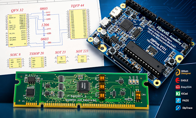
I will design schematic and pcb in altium, eagle easyeda, pads, kicad and diptrace
Circuito Impresso (PCB)
I will design flexible pcb, fpc, rigid flex pcb, schematic, footprint, gerber files

Experiência profissional

Self_employed / Freelance

PCB Design Engineer

Self employed / Freelance • Autônomo

Sep 2010 - Present16 yrs

Designed professional PCB layouts for electronic products and prototypes, with a focus on accuracy, manufacturability and clean routing. Experienced in schematic capture, component placement, PCB routing, multilayer PCB design, design rule checks, DFM optimisation, Gerber and drill file generation, BOM preparation and PCB documentation. Worked with Altium Designer, KiCad and EasyEDA to develop reliable, production-ready circuit board layouts while meeting project specifications and manufacturing requirements.