Ver categorias
Explorar
Fiverr Pro
Português
$
USD
Flexible, High Speed and Antenna PCB Design Engineer
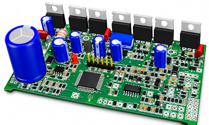
Looking for a reliable RF or microwave PCB designer? I can help turn your schematic or circuit concept into a professional, manufacturing-ready PCB.
SERVICES I OFFER
WHAT YOU WILL GET
Depending on your package: PCB design files, Gerber and drill files, BOM, schematic/layout PDFs, and impedance or stackup notes.
WHY CHOOSE ME
I focus on clean layouts, signal integrity, practical manufacturing requirements, organized files, and clear communication. I work with KiCad, Altium Designer, and compatible formats based on your project needs.
READY TO START?
Send your schematic or project concept, operating frequency, target impedance, board size, layer count, and preferred software. Contact me before ordering for complex designs or specialized requirements. Lets build your RF PCB project!
NOTE : CONTACT ME BEFORE PLACING AN ORDER!!!
What information do you need to start an RF PCB project?
I typically need your schematic or circuit description, operating frequency, target impedance, board dimensions, layer count, component information, and preferred PCB software.
Can you design 50-ohm controlled-impedance traces?
Yes. I can design for 50-ohm or other specified impedances using suitable stackup and transmission-line parameters, subject to available fabrication information.
Do you design microwave PCBs?
Yes. I can help with microwave PCB layouts based on the specified frequency range, substrate, stackup, component footprints, and design constraints.
Do you provide Gerber files
Yes. Gerber, drill, and other manufacturing outputs can be included according to the selected package.