Ver categorias
Português
$
USD
Conecte-se à sua IA

PCB Design Engineer
Habilidades
Conheça meus serviços
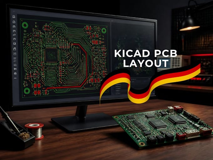
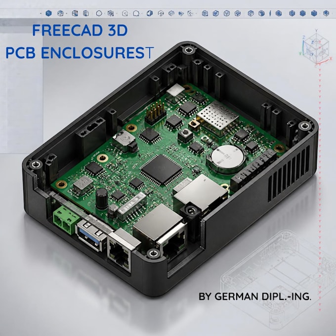

Electronic Design Engineer / PCB Layouter
Technoloy • Período integral
Aug 2021 - Mar 2026 • 4 yrs 7 mos
During my 5 years work experience, I worked on a variety of PCB and microelectronics projects. My responsibilities included designing and developing PCB layouts, component placement, routing, creating footprints, and preparing boards for manufacturing. I worked on both standard PCBs and more specialized microelectronic applications e.g. stencil printing projects. One of the larger projects I worked on was a PCB layout for a military application. My role focused specifically on the PCB layout and routing, following the required technical and design specifications. This experience gave me a strong understanding of professional PCB design, attention to detail, design constraints, and manufacturing requirements
