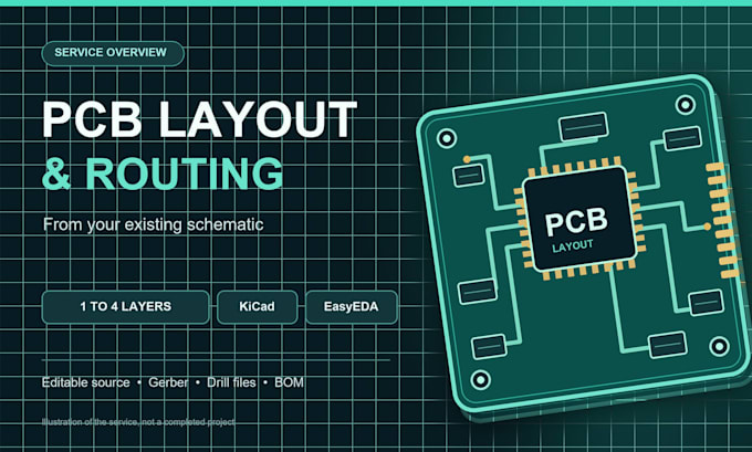
PCB Layout Designer using EasyEDA and KiCad for 1 to 4 layer boards
China
Chinês, Inglês
Algumas informações são exibidas no idioma inglês.
Sobre mim
I create 1–4 layer PCB layouts from an existing schematic using EasyEDA (JLCEDA) or KiCad. I can place components, route the board, and refine the layout around your board outline, connector positions, and manufacturing constraints. Please send your schematic and key requirements before ordering so we can agree on the scope, deliverables, and timeline. I value clear communication and will flag unclear or conflicting requirements before proceeding.... Saiba mais