Algumas informações são exibidas no idioma inglês.
Sobre mim
I am an Electronics and Communication Engineering student with practical knowledge of PCB design and layout development. I have completed a PCB Design course under the Naan Mudhalvan Scheme, Government of Tamil Nadu.
I use KiCad and EasyEDA to provide:
• PCB Schematic Design
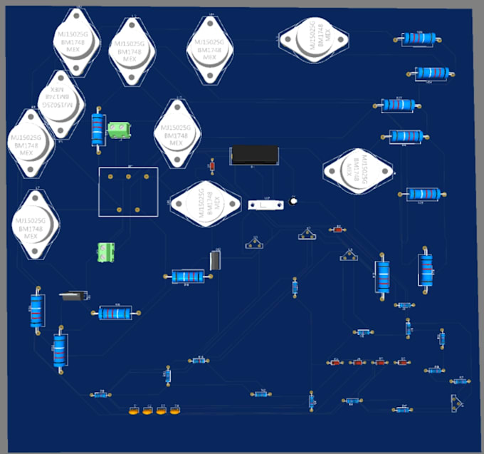
• PCB Layout Design
• Component Placement & Routing
• Gerber File Generation
• BOM Preparation
• PCB Modification
• Basic IoT & Embedded PCB Design
I focus on creating neat, reliable, and manufacturable PCB layouts based on your requirements. Let's turn your circuit ideas into reality!... Saiba mais