Ver categorias
Português
$
USD
Conecte-se à sua IA
PCB Design Circuit Design Electronics Engineering Specialist
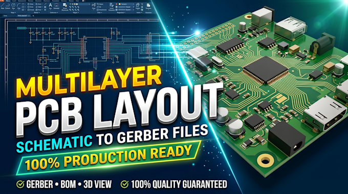
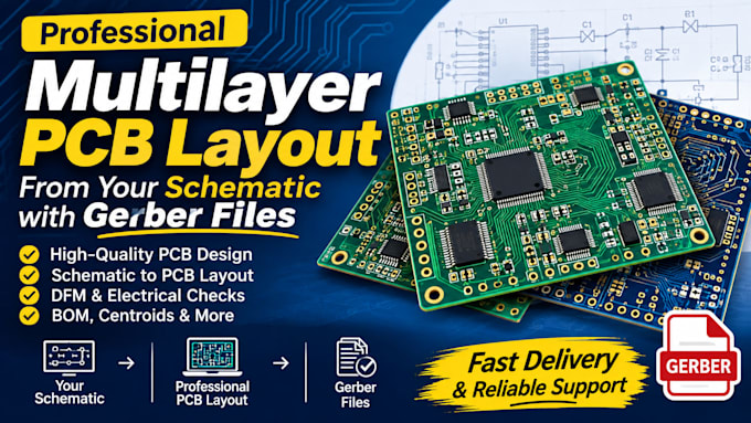
Need a reliable multilayer PCB layout that is ready for manufacturing?
I will transform your circuit schematic into a professional, well-organized PCB layout with careful component placement, optimized routing, and manufacturing-ready Gerber files.
My services cover multilayer PCB design, component arrangement, signal routing, power distribution, design rule checks (DRC), and electrical rule checks (ERC).
Depending on your project, I can also provide the PCB source files, Bill of Materials (BOM), drill files, and assembly documentation.
Whether you're developing an embedded system, microcontroller board, IoT device, or complex electronic product, I focus on accuracy, functionality, and manufacturability.
Send me your schematic and project requirements. Let's turn your circuit into a production-ready PCB design!
Can you convert my schematic into a multilayer PCB?
Yes. I can transform your supplied schematic into a structured multilayer PCB layout with component placement and routing.
Which PCB design software do you use?
I can work with your preferred supported PCB design software. Please confirm the software before ordering.
Will I receive Gerber files?
Yes. Manufacturing ready Gerber and relevant drill files are included according to your selected package.
Can you design complex PCB boards?
Yes. I can review multilayer boards involving microcontrollers, embedded systems, power circuits, and other electronic applications. Complex requirements may need a custom offer.
Can you provide the original editable PCB files?
Yes. Editable source files are included in the packages, allowing you to continue working on your design.