Algumas informações são exibidas no idioma inglês.
Sobre mim
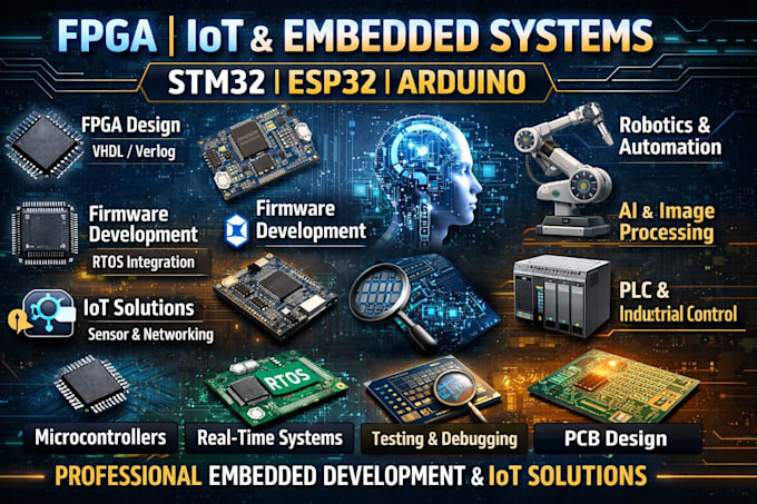
I am a professional PCB Design Engineer specializing in high-quality schematic design, PCB layout, and manufacturing-ready solutions. I design single-layer, multilayer, and high-speed PCBs using Altium, KiCad, and EasyEDA. From concept to production, I deliver optimized Gerber files, BOM, and 3D models for IoT, Arduino, ESP32, and STM32 projects. Expect fast delivery, clear communication, and reliable results that meet industry standards and boost your product success.... Saiba mais