Ver categorias
Explorar
Fiverr Pro
Português
$
USD
cole
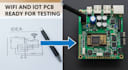
If youre building a WiFi or IoT device and your PCB keeps failing, disconnecting, or behaving unstable, the problem is usually not your codeits your board design.
Thats where I come in.
I design WiFi and IoT PCB layouts for ESP32, ESP8266, and similar wireless modules with proper routing, stable signal paths, and clean power distribution. The goal is not just to make it work but to make it stable, manufacturable, and ready for real-world use.
Whether you are working on smart home devices, sensors, automation systems, or embedded wireless products, I make sure your layout supports strong signal integrity and avoids common RF mistakes that kill performance.
If you already have a schematic, I can refine it. If you dont, I can help structure one from your idea.
Youll receive production-ready files (Gerber, BOM, and layout files) that you can send directly to manufacturers without stress or rework.

Q: Do you design ESP32 and ESP8266 boards?
A: Yes, I specialize in WiFi-based IoT modules like ESP32 and ESP8266.
Q: Will my PCB be ready for manufacturing?
A: Yes, I deliver Gerber files and production-ready outputs.
Q: Do you handle RF/antenna design?
A: Yes, I optimize antenna placement and RF routing for stable performance.
Q: Can you fix my existing PCB design?
A: Yes, I can review and improve existing layouts.
