Ver categorias
Português
$
USD
Conecte-se à sua IA
johnPcB
Are you experiencing poor wireless range, dropped signals, or failing FCC/CE certification due to bad RF layout choices? High-frequency signals do not behave like standard DC tracesthey require precision electromagnetic consideration.
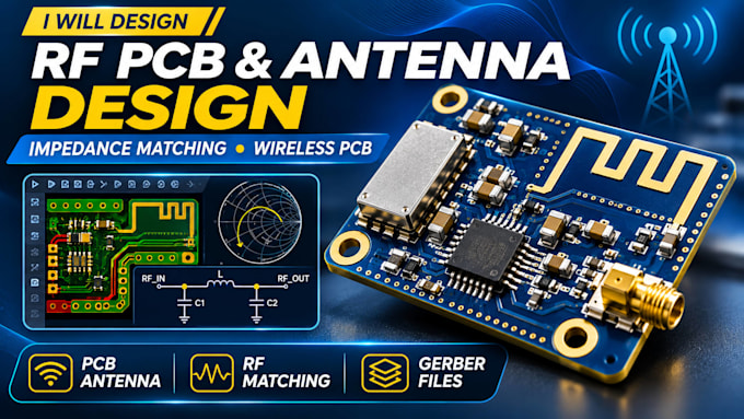
Welcome! I am a specialized RF PCB design engineer focusing on impedance matching, wireless hardware integration, and high-frequency trace routing. Whether you are using BLE, Wi-Fi, LoRa, GNSS, or sub-GHz custom transceivers, I will ensure your RF front-end achieves maximum power transfer and low return loss.
What I Specialize In:
Impedance Matching Networks: Designing Pi, T, or L networks using Smith Charts to match transceivers seamlessly to antenna
Deliverables You Receive:
Production-ready Gerber files (including custom stackup requirements).
BOM (Bill of Materials) with RF-grade high-Q inductors and tight-tolerance capacitors.
Impedance calculation reports and Smith Chart reference values.
Native EDA source files (Altium Designer, KiCAD, or Cadence Allegro).
Note: RF layouts are highly dependent on substrate material and layer stackup. Please message me with your component datasheets and manufacturing goals before ordering!
Formato de arquivo:
Gerber
•
Passo
•
3DS
•
Software:
Allegro
•
Designer Altium
•
Eagle CAD
•
KiCad
Interface:
HDMI
•
USB
•
SPI
•
I2C
•
Wi-Fi
