Ver categorias
Explorar
Fiverr Pro
Português
$
USD
Himalayan Engineering Lab Pvt Ltd
Looking for a reliable, efficient PCB designer for your next electronics project? You're in the right place.
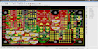
Im a professional PCB designer and embedded systems engineer with hands-on experience in KiCad for creating clean, optimized, and DFM-ready PCB layouts.
Whether you need a single-layer prototype, a multi-layer high-speed PCB, or a production-ready layout, I'll deliver precise, industry-standard designs with proper DRC and manufacturing outputs.
Custom schematics and library management
Multi-layer and high-speed PCB routing
Gerber, BOM, Pick & Place, and Drill files
Power and signal integrity optimization
Assembly-ready fabrication outputs


Can you import designs from other platforms into KiCad?
Yes — I can convert Altium, Eagle, or EasyEDA files into KiCad layouts and work from there.
Will you provide manufacturing-ready files?
Absolutely. Every project includes Gerber files, drill files, BOM, and Pick & Place for fabrication.
Do you handle high-speed and impedance controlled routing?
Yes — my Premium package covers multi-layer, high-speed boards with impedance control and via stitching.
What’s the maximum component count you support?
Up to 300 components in the Premium package. Custom quotes available for larger designs.
Can you design the schematic if I only have a circuit diagram?
Of course — just send me your circuit diagram (hand-drawn or software-generated), and I’ll convert it into a clean KiCad schematic.


