Ver categorias
Explorar
Fiverr Pro
Português
$
USD

PCB Design Specialist
Habilidades
Conheça meus serviços
PCB Layout Engineer
Systemized Business Automation - Achieve More & By Doing Less • Período integral
Nov 2024 - Present • 1 yr 6 mos
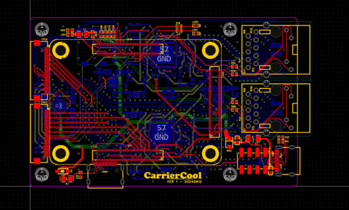
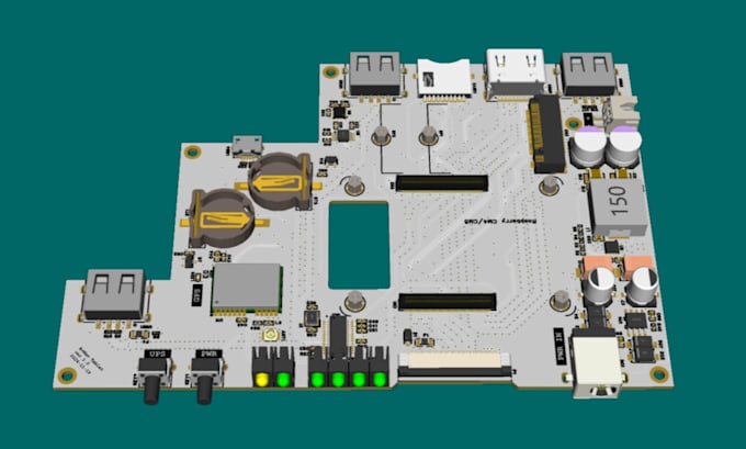
•Contract PCB Design Engineer role for start-up company developing human-machine interfaces. •Layout of PCBs using a mix of technologies such as PTH, multilayer, blind and buried vias. •PCB design for analogue, digital and power applications. •PCB layout with all Design for Manufacture (DFM) requirements considered. •Close liaison with engineering teams including hardware, mechanical, and external manufacturers. •Definition and roll-out of new workflow for PCB design. •Development of database application for PCB design management. •Standardisation of design practices, drawings and manufacturing datapacks. •Technical consultant for PCB design throughout the company. •Creation and maintenance of EDA library to IPC standards with embedded 3D models. •3D model generation for mechanical verification. •Definition of PCB specifications, layout design rules, layer build-ups and fabrication requirements. •Working with EMS companies to ensure standardised assembly data meets requirements. •Complete PCB design management and design reviews. •Comprehensive use of Altium Designer and Altium365 workspace. •Procurement of fabricated PCBs and assemblies.
PCB Design Engineer
SYSTEMIQ
Jan 2024 - Oct 2024 • 9 mos
•Contract PCB Design Engineer role for start-up company developing human-machine interfaces. •Layout of PCBs using a mix of technologies such as PTH, multilayer, blind and buried vias. •PCB design for analogue, digital and power applications. •PCB layout with all Design for Manufacture (DFM) requirements considered. •Close liaison with engineering teams including hardware, mechanical, and external manufacturers. •Definition and roll-out of new workflow for PCB design. •Development of database application for PCB design management. •Standardisation of design practices, drawings and manufacturing datapacks. •Technical consultant for PCB design throughout the company. •Creation and maintenance of EDA library to IPC standards with embedded 3D models. •3D model generation for mechanical verification. •Definition of PCB specifications, layout design rules, layer build-ups and fabrication requirements. •Working with EMS companies to ensure standardised assembly data meets requirements. •Complete PCB design management and design reviews. •Comprehensive use of Altium Designer and Altium365 workspace. •Procurement of fabricated PCBs and assemblies.
