Ver categorias
Explorar
Fiverr Pro
Português
$
USD
ELECTRONIC AND ELECTRICAL ENGINEERING
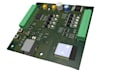
Are you struggling with weak wireless performance, poor RF range, or unstable embedded communication in your electronics project? I provide professional RF Microwave PCB design and antenna layout solutions optimized for high-frequency and embedded systems.
Expert in RF Microwave PCB Design, Antenna Layout Design, ESP32 PCB Design, STM32 PCB Design, KiCad PCB Deslgn, High-Frequency RF Layout, Impedance Controlled Routing, and Signal Integrity Optimization for reliable and production-ready results.
With strong expertise in RF and embedded hardware design, I create clean schematic-to-PCB conversions that ensure low noise, minimal EMI, and maximum signal efficiency. My designs are optimized for wireless communication systems, IoT devices, IoT modules, microcontroller-based systems, and high-speed RF applications.
I focus on precise antenna placement, proper grounding techniques, controlled impedance traces, and multilayer stack-up deslgn to guarantee stable transmission and improved performance for ESP32 and STM32-based projects.
Lets turn your idea into a high-performance RF microwave PCB deslgn that ensures stability, accuracy, and professional-grade wireless communication.

What PCB design tools do you use?
I mainly use KiCad, altium designer, easyeda and more for professional RF, microwave, and embedded PCB design projects.
Do you design ESP32 and STM32 boards?
Yes, I design optimized PCB layouts for both ESP32 and STM32-based systems.
Can you handle RF microwave and antenna design?
Yes, I specialize in RF microwave PCB design, antenna layout, impedance control, and EMI reduction.
Will I get manufacturing files?
Yes, I provide Gerber files, BOM, and full production-ready documentation.
Do you optimize for signal integrity?
Yes, all designs are optimized for low noise, stable RF performance, and high signal integrity.
