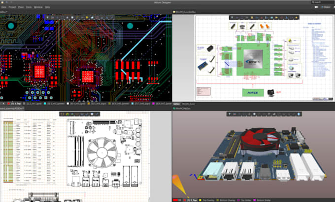
Professional PCB schematic and layout designer using Altium or KiCad
Polônia
Polonês, Inglês
Algumas informações são exibidas no idioma inglês.
Sobre mim
Hi, I am Electronics engineer specializing in PCB schematic capture and layout design. I work with Altium Designer, KiCad, Fusion 360 and other industry standard EDA tools to turn your circuit ideas into clean, manufacturable PCB designs.
I handle schematic design, component placement, routing, and design rule clean layouts for a range of projects, from simple two layer boards to more complex multi layer designs. I pay close attention to signal integrity, thermal considerations, and manufacturability (DFM) so your board works right the first time and is ready to send straight to fabrication.... Saiba mais