Ver categorias
Explorar
Fiverr Pro
Português
$
USD
logo
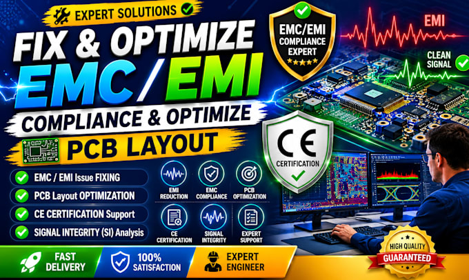
Did your electronic product fail lab testing, or are you trying to guarantee a pass on your very first try?
I provide elite EMC/EMI diagnostic and PCB layout optimization services designed to secure your CE, FCC, or CISPR certifications. I hunt down the invisible culpritsground loops, cross-talk, switching noise, and poor return pathsand rewrite your board layout for absolute electromagnetic silence.
What I Fix & Optimize For You:
Return Path Integrity: Designing solid, uninterrupted ground planes to eliminate radiating loop antennas.
High-Speed Signal Routing: Proper differential pair routing, guard ring placement, and impedance matching.
Layer Stackup Optimization: Transforming noisy 2D/2-layer chaos into quiet, self-shielding multi-layer architectures.
Component Decoupling & Filtering: Strategic placement of passives, ferrites, and TVS diodes directly at noise sources.
What You Will Receive:
A comprehensive EMC/EMI Redesign Report highlighting failure root causes and fixes.
Fully optimized, production-ready native CAD project files and Gerbers.
Direct consulting support to guide your product through the test lab smoothly.
Message me with your test reports or schematics


Do you guarantee my board will pass CE/FCC testing?
While I cannot control lab setup variables, I guarantee to implement industry-standard hardware mitigation techniques that directly target your failure frequencies to maximize your passing probability.
What files do I need to provide?
Please provide your schematic diagrams, current PCB layout files, a full Bill of Materials (BOM), and your lab test data/plots if you have already failed a simulation or test.