Ver categorias
Explorar
Fiverr Pro
Português
$
USD
Técnico em Eletrônica Desenvolvedor Frontend
POR FAVOR, ENTRE EM CONTATO COMIGO ANTES DE FAZER UM PEDIDO
Para garantir os melhores resultados e confirmar a complexidade do projeto, envie-me uma mensagem com seus requisitos antes de fazer o pedido. Vamos garantir que estamos alinhados!
O que ofereço neste serviço:
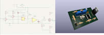
Captura do esquema (se você selecionar o serviço extra)
Roteamento e otimização de layout de PCB de 1 ou 2 camadas
Atribuição de footprint e criação de componentes personalizados, se necessário
Lista de materiais (BOM) com detalhes dos componentes
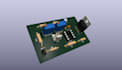
Modelo 3D da sua placa finalizada (.STEP ou imagens de visualização 3D)
Arquivos Gerber prontos para produção (compatíveis com JLCPCB, PCBWay, etc.)
Ideal para:
Projetos com Arduino, ESP32 e microcontroladores em geral
Placas de sensores e eletrônica modular DIY
Projetos de laboratório estudantil e pequenos circuitos de automação
Prototipagem e designs de hobby
Meu objetivo principal é entregar roteamento limpo, planos de terra adequados e documentação precisa.
Envie-me uma mensagem com seu esboço,

Formato de arquivo:
Gerber
•
BRD
•
SCH
•
•
Outros
Software:
KiCad
Interface:
UART
•
USB
•
SPI
•
I2C


