I will design rf pcb antenna impedance matching and wireless circuit

Algumas informações são exibidas no idioma inglês.

Reino Unido

Eu falo Inglês

edwardpcb

About Share some details about yourself, your expertise, and what you offer. Section placeholder image Skills and expertise Attract relevant clients by sharing your strengths and abilities
Sobre este Serviço

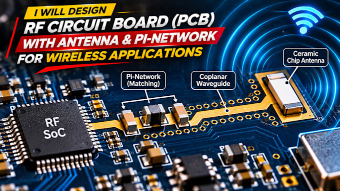
Is your custom IoT device suffering from poor Bluetooth connection range, dropped WiFi packets, or failing regulatory emissions testing? At high frequencies, a standard PCB trace behaves like a complex transmission line. Simple layout oversight can completely ruin your wireless signal integrity.

I provide expert RF PCB layout engineering, antenna impedance matching, and wireless circuit optimization designed to maximize range and achieve reliable field operation.

Instead of dealing with unpredictable signal loss, I calculate precise copper geometries and construct matching pi-networks to deliver flawless 50-ohm transmission lines straight to your antenna.

RF Problems I Solve:

  • Impedance Mismatch: Designing clean 50-ohm coplanar or microstrip waveguides.
  • Antenna Integration: Trace antenna layouts, chip antennas, and external coax connectors (U.FL / SMA).
  • Range Issues: Calculating and tuning Pi/T matching networks for optimal VSWR.
  • Niche Support: Bluetooth (BLE), WiFi (2.4GHz/5GHz), Sub-1GHz LoRa, GPS/GNSS, and Cellular IoT networks.
  • Noise Isolation: Ground plane stitching, guard traces, and custom RF shielding frames.

What You Receive:

  • Optimized layout files with calculated dielectri

Especialização:

Design de circuito

•

Representações esquemáticas

Formato de arquivo:

Gerber

•

PDF

Software:

Allegro

•

Designer Altium

•

Eagle CAD

•

EasyEDA

•

KiCad

Interface:

HDMI

•

MIPI DSI/CSI

•

USB

•

Wi-Fi

•

BT

•

LTE