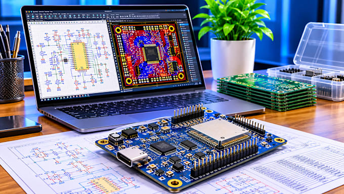
I will design ESP32 or STM32 PCB schematics, layout, Gerber, BOM and CPL files
A custom embedded device needs a carefully designed circuit, a reliable PCB layout, and accurate manufacturing files.
I design custom PCBs for ESP32, ESP32-S3, STM32, IoT devices, sensors, and embedded electronics projects
SERVICES
- Custom schematic de sign and circuit development
- PCB layout, component placement, routing
- 2-layer and multilayer PCB d esign
- ESP32, ESP32-S3, STM32, sensor and IoT boards
- Gerber, drill, BOM, CPL / Pick-and-Place files
- Design rule checks, footprint review, layout optimization
- ESP32 custom PCB
- ESP32-S3 PCB de sign
- STM32 microcontroller PCB de sign
- Custom embedded system PCB development
- IoT device PCB design
- PCB schematic capture
- Circuit diagram to PCB conversion
- Existing schematic to PCB layout
- Custom microcontroller circuit design
- Single-layer PCB layout
- Double-layer PCB layout
- 4-layer PCB design
- Multilayer PCB routing
- PCB component placement
- PCB trace routing
- PCB power supply d esign
- USB-C interface PCB
- UART, SPI, I2C, CAN interface d esign
- Sensor interface PCB de sign
- GPIO expansion board de sign
- ESP32 development board
Contact me for more information