Ver categorias
Explorar
Fiverr Pro
Português
$
USD
electrical engineering
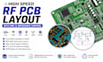
High-speed RF PCB designs failing in EMI tests, unstable signals, or poor wireless range? I will solve that with precision-engineered RF PCB layouts optimized for performance and manufacturability.
I design professional high-speed RF PCBs for LoRa, WiFi, BLE, GPS, GSM, ESP32 and IoT systems with strict impedance control and EMC compliance to ensure reliable real-world operation.
What I offer:
Tools: Altium Designer, KiCad, ADS (as required)
Why choose me:
I am focused on real engineering performance not just PCB drawing. Every design is built for stability, low noise, and manufacturability.
You are protected with clear communication, revision support, and clean deliverables.
Message me before ordering to discuss your project requirements for best result

What do you need to start my RF PCB design?
I need your schematic (or idea), required modules (LoRa, WiFi, BLE, GPS, GSM, ESP32), size constraints, and any reference design if available. If unsure, I can guide you before starting.
Will the PCB support impedance control and high-speed signals?
Yes. I design with controlled impedance (typically 50Ω RF traces), proper stack-up planning, and routing techniques to ensure signal integrity and stable RF performance.
Do you provide source files and revisions?
Yes. You will receive full production files (Gerber, BOM, Pick & Place). Revisions are included based on your package to ensure the final design meets your requirements.


