Algumas informações são exibidas no idioma inglês.
Sobre mim
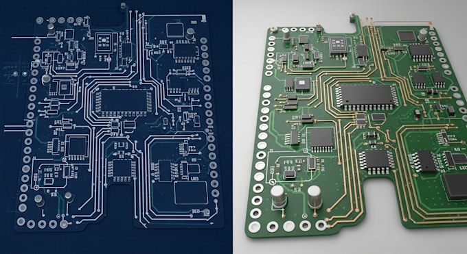
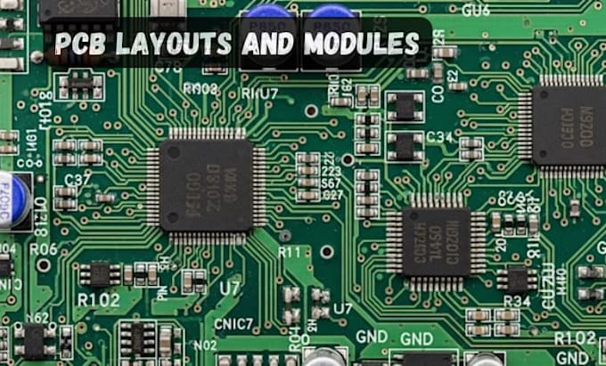
Hello, I’m Jack Bolin, a professional PCB Design Engineer specializing in schematic design, multilayer PCB layout, and manufacturing-ready files. I design high-quality, reliable, and production-ready boards using industry-standard tools. My focus is clean routing, signal integrity, proper component placement, and DFM compliance to ensure smooth fabrication and assembly. From concept to final Gerber files, I deliver accurate, optimized designs tailored to your needs. Whether it’s a simple 2-layer board or a complex design, I provide fast communication, precision, and dependable results.... Saiba mais