Ver categorias
Português
$
USD
Conecte-se à sua IA
RF PCB layout, antenna design, impedance control and wireless PCB solutions
Need a professional RF PCB for your wireless or high frequency electronic product?
I provide reliable RF PCB layout, antenna integration, controlled impedance routing, RF routing, and wireless PCB solutions optimized for signal integrity, low loss, grounding, and manufacturability.
WHAT I OFFER:
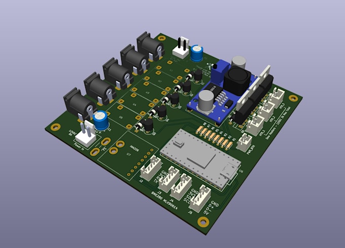
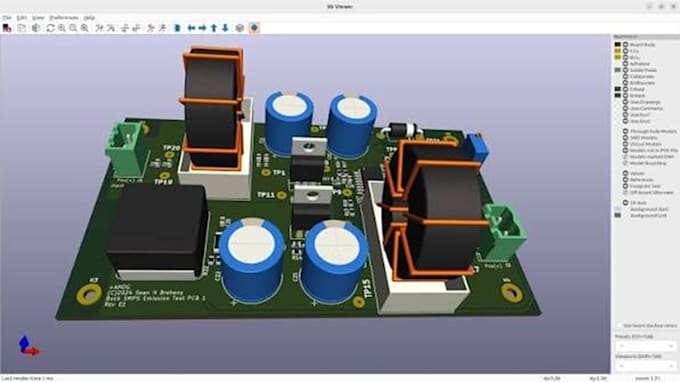
RF PCB design and high frequency PCB layout
PCB antenna design and antenna integration
Controlled impedance and RF trace routing
Impedance matching and RF optimization
Multilayer PCB layout and component placement
WiFi, Bluetooth, BLE, LoRa, GSM, GPS/GNSS and IoT hardware
Signal integrity, grounding and DFM considerations
DELIVERABLES:
Schematic and PCB layout
Gerber and drill files
BOM and Pick and Place files
PCB source files
PDF documentation and 3D PCB files
Manufacturing ready outputs
SOFTWARE USED:
Altium Designer, KiCad, EasyEDA, Eagle CAD, Cadence OrCAD and LTspice.
Whether you need an RF antenna PCB, wireless communication board, high frequency PCB, or production ready RF layout, I focus on clean routing, reliable performance and professional documentation.
Message me with your requirements before ordering.