a
adek_lab

Adekunle

@adek_lab

Pcb designer

Nigéria
Inglês, Alemão, Italiano, Espanhol
Algumas informações são exibidas no idioma inglês.
Sobre mim
Hi, I'm Adek, an Electronics and PCB Design Engineer passionate about turning ideas into reliable, manufacturing-ready circuit boards. I specialize in PCB layout, schematic design, Gerber files, BOM, and 3D PCB design using KiCad, EasyEDA, and Altium Designer. I work with startups, businesses, students, and hobbyists to deliver high-quality, optimized designs with fast communication, attention to detail, and on-time delivery. Let's bring your electronics project to life!... Saiba mais

Habilidades

a
adek_lab
Adekunle
offline • 

Conheça meus serviços

Circuito Impresso (PCB)
I will design pcb layout, schematic and gerber files using kicad and easyeda
Circuito Impresso (PCB)
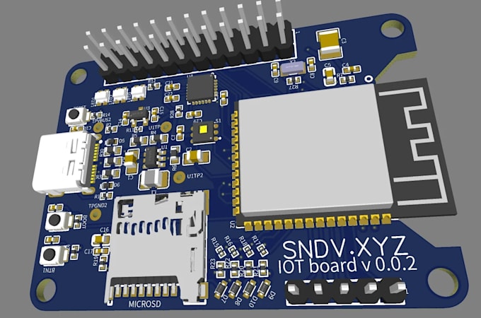
I will design esp32 arduino stm32 iot pcb layout and schematic

Experiência profissional

Freelancer.com

Electronics & PCB Design Engineer

Freelancer.com • Autônomo

Nov 2022 - Present3 yrs 8 mos

Design professional PCB layouts, circuit schematics, and manufacturing-ready electronic hardware for startups, businesses, students, and hobbyists. Create single-layer, multi-layer, and high-speed PCB designs using Altium Designer, KiCad, and EasyEDA. Generate Gerber files, BOMs, Pick-and-Place files, and 3D PCB models while ensuring DRC compliance and manufacturability. Develop ESP32, STM32, Arduino, and IoT hardware solutions, provide component selection, prototype support, and optimize designs for reliable production.